Introduction
The terms "perovskite" is usually used interchangeably. Technically speaking, a Perovskite is a type of mineral that was the first discovered In the Urals in Russia by Gustav Rose in 1839 and named after the Russian mineralogist and geographical Lev Pervski [1]. Perovskite solar cells have shown remarkable progress in recent years with significant increases in power conversion efficiency (Pce) according to reports of about 3% in 2006 to over 24% in 2019. This very high PCE is related to the excellent photo electronic properties of this material such as: direct band gap, broad absorption spectra, and high mobility of charge carriers. While perovskite solar cells have become highly efficient in a very short time and low cost, perovskite solar cells have attracted extensive attention from researchers worldwide and have developed rapidly in recent years. In other hands, a number of challenges remain before they can become a competitive commercial technology [2]. A photovoltaic perovskite is a A substance that has the same crystal structure as the titanium oxide and the mineral calcium (CaTio3) compound, which has the general molecular structure of the type ABX3, where it represents the "A" and "B" cations and X is Anion binds to cations A and B. In perovskites, the ‘A’ cation is much larger than the ‘B’ cation. Perovskites have a cubic crystal Structure [1, 3, 4].
Structure that we work on it, will be connected with semiconductor materials Aluminium gallium indium phosphide like electron transport layer and Aluminum gallium arsenide hole transport layer with different thickness and TiO2, ITO, Ag like transparent electrode layer and this is different from the other work who made the structure with spiro ometad and another semiconductor layers and we get efficiency 24.88% with FF 85.87% and we had optical and electrical properties that we satisfied for us.
1.1. The working principle of pervoskite solar cell
When the sun hit the solar cell, the perovskite layer in first absorbs photons to produce electron-hole pairs. Because the difference of exciton binding energy between several of perovskite materials, these excitons can form free electrons and holes to create a current.
Due to the low carrier recombination probabilities of CH3NH3PbI3 and other perovskite materials and the higher carrier mobility, the diffusion distance and lifetime of the carrier so long [5].
The longer diffusion distance and lifetime of carriers are the source of the outstanding of perovskite solar cells performance. Then, these free electrons and holes are collected by the electron transport material (ETM) and the whole transport material (HTM). Electrons are transferred from the perovskite material to TiO2, which is used for the ETM layers and finally collected by FTO. In the same time the holes are transferred to the HTM layer and collected by the metal electrode. Finally, the FTO and metal electrode are connected and the photocurrent is generated in the outer circuit [6].
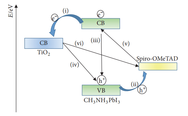
The electron-hole pairs separated at the two heterojunction interfaces of TiO2/perovskite and Spiro-OMeTAD/perovskite, followed by electrons injecting into TiO2:
Stage 1: holes injecting into HTM.
Stage 2: achieving charges transport.
Stage 3: photoluminescence, or nonradiative recombination, as well as reverse transmission of electrons and holes.
Stage 4, 5, and 6: recombination at the TiO2/HTM interface will occurs [7].
The transport processes for the electrons and holes in the HTM/perovskite/TiO2 cell are shown in figure 1.

Fig. 1. Schematic diagram of energy levels and transport processes for the electrons and holes in a HTM/ perovskite/ TiO2 cell [8]
1.2. Simulation method and structure
In order to investigate (thin film) hetero junction solar cells, a lot of different electrical measurement methods are used, ranging from standard solar cell characterization techniques like current-voltage (I-V) or quantum efficiency (EQE, IQE) to more advanced characterization techniques like for example surface photo voltage (SPV), photo- or electroluminescence (PL, EL), capacitance-voltage (C-V), capacitance-temperature C-T), impedance (IMP), or intensity modulated photocurrent spectroscopy (IMPS). We therefore developed a numerical simulation tool [10, 11].
AFORS-HET, automat for simulation of hetero structures), which allows to simulate the output of different measurement techniques for an arbitrary sequence of semiconducting layers and interfaces, with an arbitrary number of defects distributed within the different band gaps.
A user-friendly interface allows to perform multidimensional parameter variations and to visualize and analyses the corresponding results see) Different numerical modules allow treating different experimental situations, like the choice of a metal/semiconductor or a metal /insulator /semiconductor front contact [12].
1.3. Structure of pervoskit
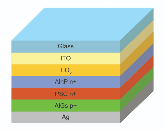
Structure that we work on it, will be connected with semiconductor materials Aluminium gallium indium phosphide like electron transport layer and Aluminum gallium arsenide hole transport layer with different thickness and TiO2, ITO, Ag like transparent electrode layer.

Fig. 2. The structure of Pervoskite
The structure dimensions would be like the simple as we explain it and for our work we will make the dimensions of ITO and Tio2 constants it would be 100 nm for both of them and for the Ag it would be 10 nm and it would be constant too but for the other layers we will change it to see in which thickness is batter efficiency with the change of the thickness of pervoskite. For the other layers table 1 will contain all information about it:
Table 1
Parameters that are used in our simulation
|
Parameters |
Alnp n+ |
PSC n+ |
AlGs p+ |
|---|---|---|---|
|
Dk – |
11.9 |
20.07 |
11.9 |
|
Chi [ev] |
3.78 |
4.1 |
3.5 |
|
Eg[ev] |
2.35 |
1.5 |
2.09 |
|
EgOp [ev] |
2.35 |
1.5 |
2.09 |
|
Nc[cm^-3] |
2x10¹⁹ |
2.5x10¹⁸ |
2x10¹⁹ |
|
Nv[cm^-3] |
2x10¹⁹ |
2.5x10¹⁸ |
2x10¹⁹ |
|
Me(n)[cm^2/Vs] |
100 |
50 |
100 |
|
Mh(np)[cm^2/Vs |
50 |
50 |
50 |
|
Na[cm-3] |
0 |
0 |
2x10¹⁸ |
|
Nd[cm^-3] |
2x10¹⁷ |
2x10¹⁷ |
0 |
|
Ve[cm/s] |
1x10⁷ |
4.4x10⁷ |
1x10⁷ |
|
Vh[cm/s] |
1x10⁷ |
1.8x10⁷ |
1x10⁷ |
|
Rho[g*cm^-3] |
2.328 |
5.32 |
2.328 |
|
Rah[cm^6/s] |
3x10-30 |
1x10-30 |
3x10-30 |
|
Rbb[cm^3/s] |
1x10⁻¹⁰ |
1x10-30 |
1x10-30 |
And as we saw the work on the AFORS program we should make the structure the same with our work and we will add all the parameters and we should be sure from the (n,k) file that we will put it for pervoskite and it would be n=2.5 and k=0.7 and it is too muvh important constants and without it the program would be crashed [13, 14, 15].
1.4. Results and Discussion
We have the parameters that we used it in table (1-1) and as the structure that we made it we will make simulation for this structure and we will calculate the best efficiency that we can get it from this structure and we will change just the thickness of layers then we will see the change in the efficiency and in any thickness and structure it would be batter, in table 2 we will see different thickness for PCS and the other layers
Table 2
Different thickness with different efficiency result
|
PSC thikness (Nm) |
Voc (mv) |
Jsc (mA/cm2) |
FF % |
η % |
|---|---|---|---|---|
|
200 |
1144 |
15.3 |
87.01 |
15.24 |
|
300 |
1138 |
17.83 |
86.83 |
17.62 |
|
400 |
1133 |
19.29 |
86.57 |
18.92 |
|
500 |
1123 |
24.25 |
85.99 |
23.64 |
|
600 |
1128 |
23.21 |
85.79 |
22.47 |
|
700 |
1124 |
22.01 |
85.62 |
21.17 |
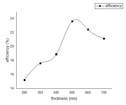
From this result we found that by changing the thickness of PCS layers and in thickness 500 Nm we will get the best efficiency from these layers and it would be 23.64 % and it is acceptable from it and we can see all the different in efficiency due to change of the thickness of pervoskite layers in figure 3.

Fig. 3. The efficiency of the structure in different thickness of pervoskite layers
And we found when we change the thickness of ALnp and make it by different thickness we found that the efficiency would be change by keeping the thickness of PCS in 500Nm as we see in table 3.
Table 3
Change on the thickness of ALnp n+
|
ALnp n+ (Nm) |
Voc (mv) |
Jsc (mA/cm2) |
FF % |
η % |
|---|---|---|---|---|
|
50 |
1135 |
25.52 |
85.87 |
24.88 |
|
100 |
1133 |
24.25 |
85.99 |
23.64 |
|
200 |
1131 |
22.66 |
86.09 |
22.07 |
From this we found that the best structure that we can get on it the best efficiency it would be when we have thickness of PCS 500Nm and the thickness of the Alnp 50 Nm and the efficiency would be 24.88%. And if we will make the simulation for laboratory situations for the same structure, we will get results would be more batter than we get it in spectra situations as we see in table 4 just we should make the order like monochromatic
Table 4
Result of simulation for laboratory state
|
ALnp n+ (Nm) |
Voc (mv) |
Jsc (mA/cm2) |
FF % |
η % |
|---|---|---|---|---|
|
100 |
1143 |
34.64 |
85.44 |
33.84 |
|
200 |
1136 |
26.97 |
85.38 |
26.31 |
Conclusion
In this project a theoretical back grounds have been considered, we covered some concepts in theoretical background relating to the optical properties of solar cell thin film materials, then we make understanding how we can make pervoskite layer worked with semiconductors layers and we considered some information about each layer that we used it and what is the goal and benefits from each one, we make understanding for advantage and dis advantage of pervoskite solar cell and how it would be the futures materials if we will get it by best quality and minimum cost with too much good efficiency and more stability.
We used simulation software program (AFORS-HET), collected information of efficiency and results of reflection and transmission the structure that we had the result for simulation of it was this structure which was prepared to be (glass/ITO/TiO2/Alnp/ CH3NH3PbI3/AlGs/Ag) and we made simulations for different thickness for pervoskite solar cell and we change the thickness for Alnp because we saw how much it can change the efficiency on the structure and we make understanding that not all layers have huge effect on the structure of pervoskite solar cell.
We made changed the structure thickness to see how it would be the effect of the thickness on the efficiency and the other parameters to make understanding for this structure and how it is work
As a result we found that there is different structures can be worked with different results and we found that the best structures was when we made the thickness of pervoskite solar cell 500Nm and the thickness of Alnp was 50 Nm and we get efficiency arrived to be 24.88% and it was too much good for this results and we saw the quantum efficiency from wave length (300-900 nm) and it was acceptable, and we saw (I-V) curve in voltage 1.2 v and in range 20 steps and we found with it the efficiency.

.png&w=640&q=75)