
Introduction
In the rapidly growing field of semiconductor manufacturing, chemical-mechanical planarization (CMP) is emerging as a key process to help achieve technological milestones in areas as diverse as cloud computing, big data technologies, 5G networks, Internet of Things (IoT), and automated systems. The global chemical mechanical planarization (CMP) market is expected to reach USD 5.4 billion in 2022. The global demand for chemical-mechanical planarization will grow at a CAGR of 5.3% over the next ten years. By 2032, the global CMP market will reach a valuation of USD 9.1 billion. This is driven by the role of CMP in creating semiconductor devices that meet the stringent requirements of advanced applications, pushing the boundaries of existing capabilities. The inherently complex CMP process involves the careful planarization and polishing of semiconductor wafers, which is a prerequisite for the sequential deposition of layers required in semiconductor fabrication. Here, a combination of chemical and mechanical principles is used, and special suspensions and overlays are applied to achieve the desired wafer surface properties [1].
As semiconductor devices shrink in size and simultaneously become more complex, the demands on the CMP process are increasing, requiring innovations that take into account new materials and architectures. The importance of CMP in this context cannot be overemphasized: it is the linchpin in device manufacturing, able to support the growing demands of today's technologies. The challenges posed by this evolution are manifold and include defect reduction, cost management, and the need for process efficiency and sustainability [2]. These challenges highlight the need for continuous research and development to optimize CMP processes. Innovations in slurry formulations and overlay technologies as well as improvements in process control are becoming critical areas of focus. These efforts are aimed at improving planarization efficiency, increasing consumable life, and reducing variability and defects while keeping in mind the environmental impact and total cost of ownership.
Thus, CMP process optimization is becoming a vital area of focus for the semiconductor industry. Addressing high material and equipment costs, energy consumption, and waste management can not only significantly reduce operating costs, but also improve the overall efficiency of semiconductor manufacturing. The purpose of this paper is to examine the current state of CMP technology, identify key cost and efficiency issues, and propose an optimization strategy. By examining materials, process improvements, and waste reduction and recycling techniques, this study aims to provide a comprehensive overview of the potential to improve the economic and environmental sustainability of the CMP process in semiconductor manufacturing.
Materials and Methods
Chemical mechanical polishing (CMP) (also called chemical mechanical planarization) is a surface-smoothing process with a combination of chemical and mechanical forces (Figure 1). It can be considered a hybrid of chemical etching and free abrasive polishing. It is used in the semiconductor industry to polish semiconductor wafers as part of the integrated circuit manufacturing process [3].
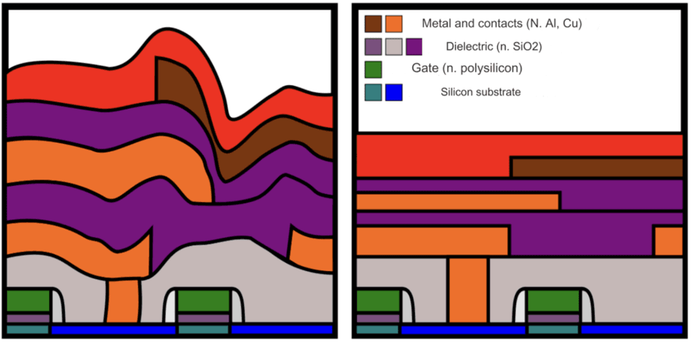
Fig. 1. Chemical-mechanical planarization
Although CMP is a planarization method that uses particles that can cause severe deflection such as scratching, it has the longest planarization length compared to existing planarization processes, making it essential for device fabrication. The main mechanism of the CMP process is the mechanical removal of chemically softened material surfaces [4]. Figure 2 shows a schematic of the CMP process and the material removal mechanism. The plate and polishing pad are attached to the underside of the holder and the shaft, respectively. A slurry containing abrasive particles and chemicals is fed to the polishing pad. The polishing head presses the plate against the pad surface. The plate and polishing plate rotate counterclockwise, causing the slurry to hit the interface between them. Pad conditioning is accomplished by using a diamond disk to clean and control the pad surface [4].
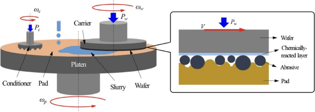
Fig. 2. Functional principle of CMP
CMP is used for global surface planarization in semiconductor fabrication such as small key insulation (STI), interlayer dielectric (ILD) planarization, tungsten (W) contact formation, and metal wiring formation. The related market is growing significantly with the increasing demand for faster and better electronic equipment such as smartphones and artificial intelligence devices [5].
Performance evaluation of the chemical-mechanical planarization (CMP) process focuses on several key performance indicators that collectively reflect the efficiency, uniformity, and integrity of the CMP process. Understanding these factors is critical to optimizing CMP protocols and achieving desired wafer surface characteristics:
- Material removal rate (MRR) is the amount of material removed from the wafer surface per unit time, usually expressed in angstroms per minute (Å/min). MRR is a critical factor in the CMP process because it directly affects the productivity and efficiency of semiconductor manufacturing. A higher MRR indicates a more efficient material removal process, which contributes to shorter cycle times and higher productivity.
- Within-wafer non-uniformity (WIWNU) measures the uniformity of material removal on a single wafer. It is defined as the variation in material thickness or surface topography within a single wafer after the CMP process.WIWNU is a critical parameter for ensuring the functional reliability of semiconductor devices because significant variation within a wafer can lead to defects in circuits and negatively impact device performance.
- Wafer-to-wafer non-uniformity (WTWNU) evaluates the consistency of material removal across multiple wafers processed under identical CMP conditions. WTWNU indicates repeatability and control of the CMP process from one wafer to the next. A high WTWNU can indicate process variability, potentially resulting in yield loss and reduced production efficiency.
- Chemical and physical defects are defects that have appeared on the wafer surface during the CMP process. These defects can include scratches, pits, corrosion, and contaminants that can compromise the electrical performance and reliability of the finished semiconductor devices. Chemical defects often result from unfavorable reactions between the wafer surface and the CMP slurry, and physical defects are usually related to mechanical interactions between the wafer, polishing pad, and abrasive particles in the slurry [6].
All these factors serve as critical metrics for evaluating the efficiency of the CMP process. Optimizing these parameters is fundamental to developing semiconductor manufacturing, enabling devices with higher performance, reliability, and miniaturization.
The selection and use of materials in chemical-mechanical planarization (CMP) – particularly slurries and polishing substrates - play a key role in determining the efficiency, cost, and environmental impact of the process. Conventional materials used in CMP are designed to meet the stringent requirements of semiconductor manufacturing, including achieving ultra-smooth surfaces, minimizing defects, and maintaining process uniformity across materials (e.g., oxide, metal, and polysilicon layers).
The materials used in the slurries (Figure 3) are critical to achieving the desired surface quality and material removal rates required for semiconductor manufacturing.
Fig. 3. The main constituents of CMP
The main materials used in CMP suspensions include aluminum oxide (Al2O3), silica (SiO2), cerium (CeO2) and zirconium dioxide (ZrO2). These materials are chosen because of their abrasive properties, which are necessary for leveling and polishing semiconductor wafers:
- Alumina (Al2O3): known for its hardness and durability, aluminum oxide is often used in CMP slurries to polish hard materials. It offers excellent removal rates and is particularly effective for applications that require significant material removal or for hard surface treatment. The alumina segment accounts for the highest market share of 39% in the overall chemical mechanical planarization (CMP) slurries market in 2021 (Figure 2).
- Silica (SiO2): Silica is widely used in CMP suspensions due to its relatively mild abrasive action, making it suitable for leveling softer materials and for applications where minimal damage to the substrate is critical. Its chemical inertness and the availability of various particle sizes provide a high degree of process customization.
- Cerium (CeO2): Cerium is valued not only for its mechanical abrasive properties but also for its chemical activity. It is particularly effective for polishing oxide layers due to its ability to react chemically with the surface, increasing removal rates and improving surface quality.
- Zirconium (ZrO2): Zirconium is used in CMP suspensions because of its exceptional hardness and chemical stability. It is suitable for polishing very hard surfaces and is often used where aggressive material removal with minimal abrasive particle wear is required [3].
The choice of a particular abrasive material is determined by several factors, including the material to be polished, desired surface finish, removal rate, and overall process compatibility. Each abrasive material has certain advantages: aluminum oxide and zirconium provide high removal rates for hard materials, silicon dioxide provides softer abrasion for delicate surfaces, and cerium provides improved performance due to chemo-mechanical action. However, the zirconium segment is projected to be the fastest-growing segment during the forecast period (Figure 4). This is attributed to increasing R&D activities for the implementation of zirconia in chemical mechanical planarization (CMP) slurry on a global level, which is contributing to segmental growth.
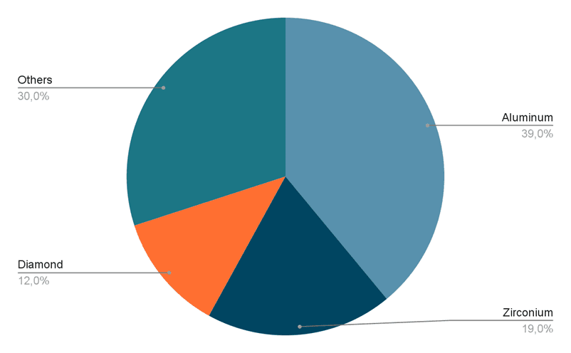
Fig. 4. Chemical Mechanical Planarization (CMP) Market by Grain Type
Recent trends in CMP materials also focus on the development of composite particles and fine-tuning of suspension formulations to achieve optimal performance. Lee and Sung [8] summarized the research topics related to CMP over the past 5 years in Elsevier DB and Springer DB (243 articles in 64 journals) (Fig. 5). Of the total number of studies, about 71.2% of the studies focus on process analysis as well as chemical and mechanical effects, and most of the studies aim to understand the mechanisms of material removal and improve the efficiency of CMP. However, recent changes in the global climate environment have increased interest in the sustainability of the semiconductor and CMP industries. Researchers are also conducting research on various methods to assess the environmental impact of semiconductor processes and reduce the environmental load. In addition, there is a growing interest in improving process efficiency to reduce energy consumption in semiconductor processes.
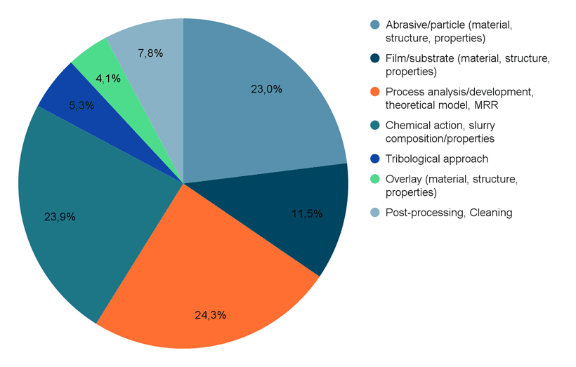
Fig. 5. CMP research topics over 5 years
The following section will discuss the environmental impact of the CMP process and the results of various studies aimed at improving sustainability, and present the future of CMP technology development.
Results
Optimizing the use of slurry and improving slurry injection systems in chemical mechanical planarization (CMP) processes have become crucial because of their significant environmental impact and the need for high reliability in semiconductor manufacturing. As the industry moves toward ever smaller gate sizes, in the future shrinking from a few tens of nanometers to a few nanometers, the accuracy and integrity of CMP results become increasingly important. This transition requires a reevaluation of the practice of reusing or recycling liquid suspension, which has historically faced challenges due to the stringent quality requirements of CMP results [9].
CMP slurry consumption is projected to increase with the number of process steps, highlighting the need to develop strategies to minimize slurry use without compromising process efficiency. Given that the slurry contains abrasive particles suspended in solution, the environmental impact goes beyond the CMP process and includes CO2 emissions associated with the production and utilization of these particles [10]. Consequently, there is a growing interest in developing slurries with lower abrasive concentration or even developing abrasive-free slurries to mitigate the environmental impact while maintaining process efficiency.
To reduce overall slurry consumption, it is important to optimize flow rates and minimize polishing time without sacrificing the quality of CMP results. Strategies to mitigate the environmental impact of suspensions include increasing the material removal rate (MRR) by improving chemical reactions and mechanical action, using reduced abrasive content suspensions or abrasive-free formulations, improving polishing uniformity to eliminate additional polishing time, and improving suspension efficiency [11].
However, increasing MRR by changing the slurry composition has its limitations in terms of reducing environmental impact. The choice of slurry components must carefully balance the environmental considerations associated with slurry use and the efficiency gains from increasing MRR. Innovations such as mixed abrasive slurry (MAS) technology, which utilizes a combination of different types of abrasives such as SiO2, Al2O3, CeO2, ZrO2, TiO2, and MnO2, have shown promising results in improving mechanical material removal. Studies have shown that MAS can achieve higher MRR and selectivity without the addition of chemical additives [12]. These results indicate that MAS can not only improve MRR and surface cleanliness but also contribute to environmental sustainability by reducing the amount of abrasive material required.
The mechanisms underlying the effectiveness of MAS include interactions between particles of different sizes and shapes. Larger particles can be coated by smaller particles due to charge differences, or they can independently promote material removal and improve surface quality [13]. This dual action provides a more efficient material removal process while minimizing surface roughness, thus aligning with the dual goal of improving process efficiency and reducing environmental impact.
Table
CMP studies on MAS and target materials [9-13]
|
MAS |
Target material |
|---|---|
|
Al2O3 + SiO2 |
Cu, Ta, SiO2 |
|
SiO2 + TiO2 |
Ba0.6Sr0.4TiO3 |
|
SiO2 + ZrO2 |
SiO2 |
|
SiO2 (large) + SiO2 (small) |
SiO2 |
|
SiO2 + SiO2 (different forms) |
SiO2 |
|
SiO2 + CeO2 or SiO2 coated with CeO2 |
SiO2 |
|
Diamond + SiO2 |
SiC |
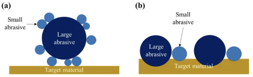
Fig. 6. MAS CMP mechanisms [10, 11]
In the field of chemical-mechanical planarization (CMP), the dual goals of increasing material removal rate (MRR) and reducing surface defects such as scratches have led to a shift towards innovative methodologies. One such advancement is the development of abrasive-free CMP (AF-CMP) methods, which have gained traction due to their environmental benefits and ability to improve CMP results. The depletion of natural abrasive particle resources and subsequent environmental concerns have accelerated AF-CMP research, highlighting its potential to reduce wafer surface damage and optimize post-CMP cleaning processes [14].
AF-CMP utilizes chemical reactions to remove material, as opposed to traditional methods based on physical abrasion. This approach significantly reduces the likelihood of scratches and eliminates common defects such as notches and erosion, thereby improving wafer surface integrity. For example, studies have demonstrated the effectiveness of using specific dicarboxylic acids as complexing agents in AF-CMP solutions for copper, with oxalic acid and malonic acid showing promising results in achieving high MRR [15]. Similar studies have investigated the use of glycine as a corrosion inhibitor in AF-CMP solutions for molybdenum, demonstrating the versatility of AF-CMP for different materials.
Furthermore, the concept of catalyst-assisted preferred etching (CARE) for SiC substrates introduces a new abrasive-free planarization method that uses a solid platinum cushion as a catalyst, offering an alternative to conventional polyurethane substrates [16]. This innovation not only means avoiding the use of abrasives but also emphasizes the environmental benefits and efficiency improvements achievable with AF-CMP.
The effectiveness of CMP is determined not only by the choice of slurry or method but also by optimizing the use and distribution of slurry. The correlation between slurry flow rate and inhomogeneity within the wafer (WIWNU) suggests that minimizing polishing time and slurry usage without compromising flatness is paramount. High-performance multi-zone membrane designs and advanced slurry delivery systems, such as sickle or spray nozzles, have been developed to provide uniform slurry distribution and pressurized slurry delivery [16]. These innovations aim to reduce slurry consumption and improve device performance by addressing the important WIWNU problem.
In particular, spray nozzle methods have demonstrated the ability to achieve higher MRR and lower WIWNU with less slurry usage compared to conventional methods. This approach, along with crescent-shaped slurry injection systems and technologies that ensure uniform slurry distribution around retaining rings, exemplify the ongoing efforts to improve CMP processes. These advances not only help reduce environmental impact and resource consumption but also improve semiconductor manufacturing accuracy and efficiency, which is in line with the industry's sustainability and innovation goals [17].
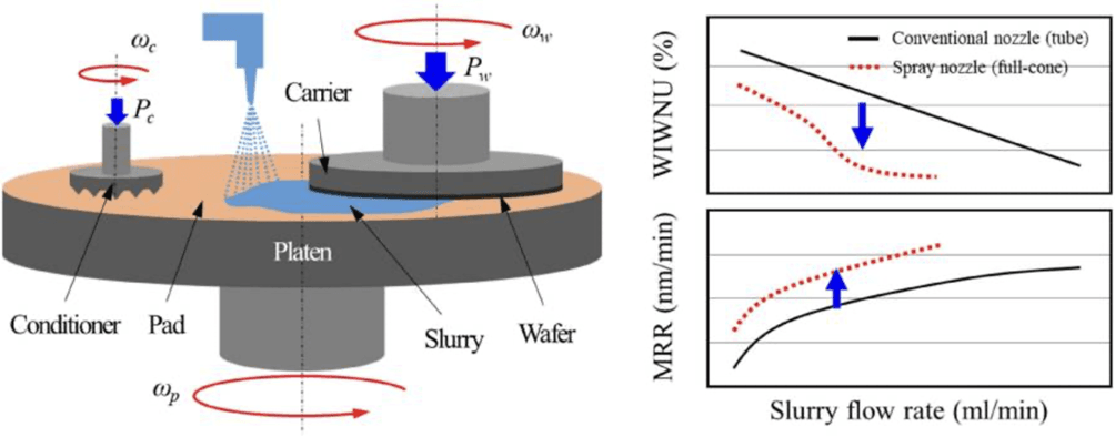
Fig. 7. Schematic diagram of CMP using spray slurry nozzle [16]
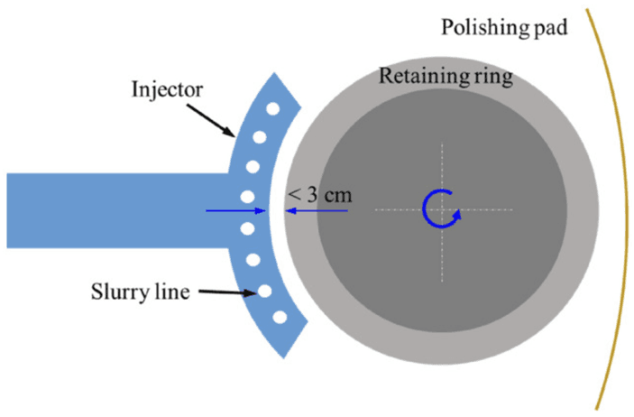
Fig. 8. Schematic diagram of slurry injection system [17]
Discussion
The challenges associated with the reuse and recycling of sludge emphasize a critical aspect of CMP - the need for reliability and integrity in semiconductor processes. As gate sizes continue to shrink, achieving this reliability becomes increasingly difficult, especially due to the stringent quality requirements of today's semiconductor devices. The discussion extends to innovative strategies to optimize suspensions without compromising process integrity, such as increasing material removal rate (MRR) through chemical and mechanical means, using non-abrasive suspensions, and improving polishing uniformity to reduce additional polishing time.
Mixed abrasive suspensions (MAS) represent a notable advancement as they utilize the effect of different abrasive materials to achieve higher MRR and better selectivity. The present research illustrates the potential of MAS to address the limitations of single abrasive slurry (SAS), providing improved efficiency and surface quality for a variety of materials. This approach not only emphasizes the importance of abrasive material selection in CMP but also highlights the innovative ways that are being explored to overcome the limitations of conventional slurries.
Also, the study of abrasion-free CMP (AF-CMP) techniques is becoming a promising area of research, especially for metallic CMP, which relies heavily on chemical reactions for material removal. The environmental benefits of AF-CMP, coupled with its ability to reduce defects such as sloughing and erosion, emphasize its importance in the context of sustainable manufacturing practices. Nevertheless, the transition to AF-CMP requires careful evaluation of its impact on process efficiency and device quality, especially in light of the chemical complexities involved.
Moreover, the correlation between slurry utilization and in-wafer heterogeneity (WIWNU) represents a critical area for discussion. The desire for an ideal CMP process with minimal WIWNU and optimized slurry usage highlights the difficult balance required between process parameters and material characteristics. Innovations in slurry delivery methods, such as spray nozzle systems and crescent-shaped slurry injection systems, are illustrative of ongoing efforts to improve CMP efficiency while minimizing environmental impact.
When discussing these advances, it is important to consider the broader implications for semiconductor manufacturing, especially in terms of cost, environmental sustainability, and process thresholds of current and future device architectures. The intersection of materials science, chemical engineering, and process optimization in CMP highlights the interdisciplinary approach required to address the challenges posed by the ongoing evolution of semiconductor devices. As the industry evolves, the dialog between research, innovation, and practical applications will remain crucial in overcoming the complexities of CMP in the quest for more efficient, sustainable, and high-performance semiconductor manufacturing processes.
Conclusion
In conclusion, advances in chemical-mechanical planarization (CMP) processes highlight a decisive shift towards achieving higher efficiency and sustainability in semiconductor manufacturing. The exploration and implementation of innovative CMP methodologies, such as non-abrasive techniques and the use of composite particles, represent a forward-thinking approach to addressing the complex requirements of modern semiconductor manufacturing. These innovations not only promise to increase material removal rates and improve surface integrity but also open the door to environmentally responsible manufacturing. By reducing reliance on abrasive materials and optimizing process parameters, the semiconductor industry can significantly reduce environmental impact while maintaining the high standards of device performance and reliability required by new technologies.
Furthermore, this study emphasizes the importance of interdisciplinary research in advancing CMP technologies. The integration of chemical and mechanical principles coupled with an increased focus on sustainability illustrates the dynamic nature of semiconductor manufacturing research. As the industry moves toward ever smaller device geometries and more complex architectures, the role of optimized CMP processes in ensuring device quality and performance becomes increasingly important. Ongoing research into new CMP strategies and materials is essential to keep pace with the rapid evolution of semiconductor technology, reinforcing the need for continuous innovation and adaptation in this area. This work contributes to the body of knowledge by providing a comprehensive analysis of current trends and potential future directions in CMP, offering insights that can guide future research and development in semiconductor manufacturing.
